| Author |
Message |
elmegil

Joined: Mar 20, 2012
Posts: 2177
Location: Chicago
Audio files: 16
|
 Posted: Sat Apr 22, 2017 10:07 pm Post subject:
CD4029 based sequencer skipping 0 Posted: Sat Apr 22, 2017 10:07 pm Post subject:
CD4029 based sequencer skipping 0 |
  |
|
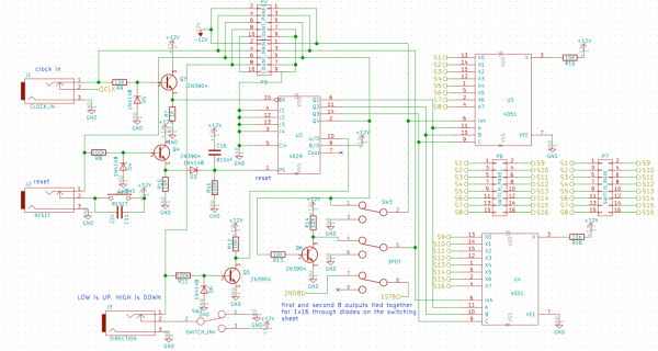
I'm working on a trigger/gate sequencer.
First rule of responses: don't tell me I ought to be using (insert your favorite programming platform), because I don't want this to be something people have to flash/program, and I don't want it to be something I have to supply programmed chips for. It's nice if you don't think that's an impediment, but some people still do and I want to include them if this thing ever gets to the "selling it from Synthcube" stage.
Design points:
Variable duty cycle output, so we can sequence triggers to gates.
Up/Down control
Ability to use it for 16 steps or 2x8 steps
CVs (gates, really) over all these controls
Clock out/clock in so you can chain several of them
Up/Down led me to the CD4029
Intent to generate variable duty cycle via AND with step gates led me to a variable duty cycle clock -- 555 for the basic clock, use the triangle buffered and run through a comparator to get the duty cycle.
Using 2 x 4051 to decode the counter into either 8 steps, or using the high bit of the clock and its inverse to alternate the two for 16 steps.
Initial problem was my clock was using an LM311 for the comparator, and only getting 0->6V, when it needed to be 10-12V for the high side.
Revised the comparator to use an LM358 (single supply config) and I'm getting a decent clock out of it.
What is weird is that from the start, when the counter was working, it was skipping steps. Counting up it would skip 0 and 8, counting down it would skip 4 and 12.
After adding a transistor buffer on the clock input, I'm no longer skipping 8 when counting up, nor am I skipping anything when I count down. But I am still skipping 0 when counting up.
So other relevant things....
the jam inputs are all grounded, as is carry in.
the load jam inputs ("PE") pin is connected both to a power on reset (cap to +V, resistor to ground) and to a diode coming from the reset input which is transistor buffered and normalled to a reset button. Pressing the reset button gets the expected result of resetting to 0 (and always has).
The schematic is something of a problem, it's actually split over multiple sheets, but the relevant bit with the 4029 is here.
I am simply not grasping why it would skip step 0. There's nothing odd about the clock as far as I can tell, for testing it's on its own power supply all alone...... Hoping someone with more CMOS experience can point to something. Speaking of which, all chips have 100nF bypass caps near their power pins.
| Description: |
|
| Filesize: |
192.14 KB |
| Viewed: |
928 Time(s) |
| This image has been reduced to fit the page. Click on it to enlarge. |
|
|
|
|
Back to top
|
|
 |
elmegil
Joined: Mar 20, 2012
Posts: 2177
Location: Chicago
Audio files: 16
|
| Posted: Sat Apr 22, 2017 10:12 pm Post subject:
|
|
|
Oh, and ignore the headers at the top; this was an experiment in how I could indicate mating headers between two boards -- controls and a little bit of support stuff is on a panel PCB, the main logic is on its own PCB. I hate the way this looks, it only made sense when I was first drawing it, and I just haven't gone back to revise it.
Overall this is going to go through a lot of serious revision (changing the switches, which also means changing to do something else instead of a 3 pole switch, they don't apparently make those in submini). But I want to get all the stupid mistakes resolved before I do that.....
And yes, I have realized I have no Run/Stop  |
|
|
Back to top
|
|
|
Grumble

Joined: Nov 23, 2015
Posts: 1294
Location: Netherlands
Audio files: 30
|
| Posted: Sun Apr 23, 2017 2:09 am Post subject:
|
|
|
By "skipping" you mean the outputs of the 4029, or the outputs of the 4051?
I mean: where did you noticed the skipping?
Because if you say that the skipping occurs at some point at 0,8,4 and 12 it's common nominator is Q4 of the 4029, so my guess is that there is something wrong with it (bad solder, shortcut ...) |
|
|
Back to top
|
|
|
PHOBoS

Joined: Jan 14, 2010
Posts: 5609
Location: Moon Base
Audio files: 705
|
| Posted: Sun Apr 23, 2017 2:46 am Post subject:
|
|
|
A resistor from the base of Q4 to GND might help. I had some problems with skipping
when using a resistor that was too large and you don't have one at all. I wasn't using
the transistors as an emitter follower though, but I think it's worth a try. btw. If you use
them like this it will most likely not work with 5V gate/triggers signals.
_________________
"My perf, it's full of holes!"
http://phobos.000space.com/
SoundCloud BandCamp MixCloud Stickney Synthyards Captain Collider Twitch YouTube |
|
|
Back to top
|
|
|
Grumble
Joined: Nov 23, 2015
Posts: 1294
Location: Netherlands
Audio files: 30
|
| Posted: Sun Apr 23, 2017 4:47 am Post subject:
|
|
|
Why not use the same resistor values around Q4 as with Q? (that's the Q with the question mark  |
|
|
Back to top
|
|
|
gdavis
Joined: Feb 27, 2013
Posts: 359
Location: San Diego
Audio files: 1
|
| Posted: Sun Apr 23, 2017 10:18 am Post subject:
|
|
|
Sorry I don't have time to read everything and go into detail right now, but I really don't think you should be using emitter-followers to buffer the inputs of the CMOS chips. And the diode on reset makes things even worse and seems completely superfluous. Anyway, I can explain more later if you want.
_________________
My synth build blog: http://gndsynth.blogspot.com/ |
|
|
Back to top
|
|
|
gdavis
Joined: Feb 27, 2013
Posts: 359
Location: San Diego
Audio files: 1
|
| Posted: Sun Apr 23, 2017 1:46 pm Post subject:
|
|
|
OK, I took another look and your inputs are seriously flawed. There's absolutely no way this thing can be expected to work reliably.
1. As I mentioned above, you don't want to use emitter-followers for logic. The output of the emitter-follower is going to follow the input voltage but lose one diode drop through the base-emitter junction (about 0.6V). So for a high input at best you get Vin - 0.6V (reset is even worse with the extra diode). The problem is that CMOS logic really wants to be driven by Vdd and Vss for high and low respectively (as close as you can get to this). so a) your clock input needs to be very specific and b) you don't want to be giving up that diode drop.
Edit: Disregard point 2. This analysis is incorrect.
2. The base and emitter resistors of Q? and Q4 (you really should annotate your schematics before posting them for help) are forming voltage dividers in addition to the drop of the emitter follower. With the values shown, you are reducing the input by about 1/10. This is going to kill the circuits ability to operate properly, especially on the clock.
3. Your reset input is floating when there's nothing connected and the button isn't being pressed. Add a pull down before the transistor base.
I would suggest replacing the emitter followers with common emitters like Q5 and Q6. Then you know you are getting the correct voltages to the CMOS inputs regardless of the external input voltages, as long as they cleanly cross the threshold of the transistor.
I also don't see the need for R41, C16 and D3. I'm guessing you're trying to extend the reset pulse? Are you worried that your reset source is going to generate too quick of a pulse?
Edit: I just read your explanation of the reset. Not sure it's going to work reliably, might work well enough. I don't see it as critical so I'm not worried about it, but you should fix the input as explained above.
_________________
My synth build blog: http://gndsynth.blogspot.com/
Last edited by gdavis on Tue Apr 25, 2017 12:05 pm; edited 1 time in total |
|
|
Back to top
|
|
|
elmegil
Joined: Mar 20, 2012
Posts: 2177
Location: Chicago
Audio files: 16
|
| Posted: Sun Apr 23, 2017 9:23 pm Post subject:
|
|
|
| Grumble wrote: | By "skipping" you mean the outputs of the 4029, or the outputs of the 4051?
I mean: where did you noticed the skipping?
Because if you say that the skipping occurs at some point at 0,8,4 and 12 it's common nominator is Q4 of the 4029, so my guess is that there is something wrong with it (bad solder, shortcut ...) |
Many thanks to the E-M alerting system which hasn't bothered to notify me of any of you folks' kind responses.
I notice it on the outputs of the 4029. I can clearly see that Q1 is not outputting a normal evenly-spaced up/down waveform as I would expect for the LSB of a binary counter. |
|
|
Back to top
|
|
|
elmegil
Joined: Mar 20, 2012
Posts: 2177
Location: Chicago
Audio files: 16
|
| Posted: Sun Apr 23, 2017 9:42 pm Post subject:
|
|
|
| gdavis wrote: | OK, I took another look and your inputs are seriously flawed. There's absolutely no way this thing can be expected to work reliably.
1. As I mentioned above, you don't want to use emitter-followers for logic. The output of the emitter-follower is going to follow the input voltage but lose one diode drop through the base-emitter junction (about 0.6V). So for a high input at best you get Vin - 0.6V (reset is even worse with the extra diode). The problem is that CMOS logic really wants to be driven by Vdd and Vss for high and low respectively (as close as you can get to this). so a) your clock input needs to be very specific and b) you don't want to be giving up that diode drop.
|
So I had two points in doing this.
1) first, trying to make sure I protect from the possibility of an incoming -12V signal off the jacks, always a possibility with random LFOs being patched in as clocks (though yes, 90% of the time -5V is most likely the lowest).
2) before I added the transistor Q?, I was getting *worse* results. At that point it was just the resistor and diode for -V protection. Edit: on the clock.
| gdavis wrote: |
2. The base and emitter resistors of Q? and Q4 (you really should annotate your schematics before posting them for help) |
Apologies, these are "in progress" and I just bodged that transistor onto the PCB about 4 hours before I posted asking for help, and the transistor into the schematic probably only a few minutes.
| gdavis wrote: | | are forming voltage dividers in addition to the drop of the emitter follower. With the values shown, you are reducing the input by about 1/10. This is going to kill the circuits ability to operate properly, especially on the clock. |
That makes sense; I'm curious why it works at all though then....
| gdavis wrote: | | 3. Your reset input is floating when there's nothing connected and the button isn't being pressed. Add a pull down before the transistor base. |
Assuming I leave the transistor there? 
| gdavis wrote: | | I would suggest replacing the emitter followers with common emitters like Q5 and Q6. |
Except those are inverting the signal. Not what I want on Q? and Q4. (it has somehow become Q1 since I annotated it, not sure where the original Q1 went ) Do I need to use PNPs and a slightly different setup then? I'm less confident in my PNP transistor knowledge than I am with NPNs 
| gdavis wrote: | Then you know you are getting the correct voltages to the CMOS inputs regardless of the external input voltages, as long as they cleanly cross the threshold of the transistor.
I also don't see the need for R41, C16 and D3. I'm guessing you're trying to extend the reset pulse? Are you worried that your reset source is going to generate too quick of a pulse? |
The resistor and capacitor are there for power on reset. Diode was intended to isolate that function from the incoming signal, but I see how it's probably entirely redundant. I do understand the cap & resistor are not a perfect solution, but it's a common enough one that I figured it should work, and I haven't noticed it ever coming up in any state but 0 to begin with.
| gdavis wrote: | | Edit: I just read your explanation of the reset. Not sure it's going to work reliably, might work well enough. I don't see it as critical so I'm not worried about it, but you should fix the input as explained above. |
It's preferred to the counter coming up in a random state. If there's a better solution I would certainly be interested in what you would recommend. |
|
|
Back to top
|
|
|
elmegil
Joined: Mar 20, 2012
Posts: 2177
Location: Chicago
Audio files: 16
|
| Posted: Sun Apr 23, 2017 9:51 pm Post subject:
|
|
|
| gdavis wrote: | | 2. The base and emitter resistors of Q? and Q4 (you really should annotate your schematics before posting them for help) are forming voltage dividers in addition to the drop of the emitter follower. With the values shown, you are reducing the input by about 1/10. This is going to kill the circuits ability to operate properly, especially on the clock. |
So further clarification on this.
I'm not sure I understand how/why the presumed divider is relevant, because I'm using the transistor as a buffer. As I understand it, I'm driving it into saturation (hopefully) and so it should be behaving as if I just threw 12V onto that line, and the 1K is to keep me from shorting my supplies together (note elsewhere I've mostly been using 10K for the same purpose, but again, experimenting with the circuit to see if anything works better, that seemed to be better). |
|
|
Back to top
|
|
|
elmegil
Joined: Mar 20, 2012
Posts: 2177
Location: Chicago
Audio files: 16
|
| Posted: Sun Apr 23, 2017 10:01 pm Post subject:
|
|
|
| PHOBoS wrote: | A resistor from the base of Q4 to GND might help. I had some problems with skipping
when using a resistor that was too large and you don't have one at all. I wasn't using
the transistors as an emitter follower though, but I think it's worth a try. btw. If you use
them like this it will most likely not work with 5V gate/triggers signals. |
As in my previous clarification question, since my goal is to drive the transistor into saturation (and no, I haven't done the math, sloppy me), as long as I have enough signal to turn on the transistor, would it matter?
I do see where I probably need to drop those other 100K input resistors down though.... |
|
|
Back to top
|
|
|
elmegil
Joined: Mar 20, 2012
Posts: 2177
Location: Chicago
Audio files: 16
|
| Posted: Sun Apr 23, 2017 10:08 pm Post subject:
|
|
|
a 10K pulldown on Q4 and eliminating D3 was insufficient.
I will see whether additional replies help me understand better before I go poking around with random values though....
Again: thanks very much for all the replies. I have a degree, but I was never very good with transistors (obviously ), and that degree didn't get used in any practical way for 25 or so years, so even what I did know is all pretty rusty where it hasn't been polished by actual use troubleshooting other circuits..... |
|
|
Back to top
|
|
|
PHOBoS
Joined: Jan 14, 2010
Posts: 5609
Location: Moon Base
Audio files: 705
|
| Posted: Mon Apr 24, 2017 4:29 am Post subject:
|
|
|
| elmegil wrote: | | As in my previous clarification question, since my goal is to drive the transistor into saturation (and no, I haven't done the math, sloppy me), as long as I have enough signal to turn on the transistor, would it matter? |
As the name suggest with an emitter follower the voltage on the emitter follows the voltage at the base,
so 5V in gives you about 5V out but with a low impedance. I would suggest using comparators (made with
opamps) for the CLK and reset inputs. PNP transistors would still invert, be it the other way aroud, so you'd
need a negative/low voltage on the inputs or an extra transistor.
_________________
"My perf, it's full of holes!"
http://phobos.000space.com/
SoundCloud BandCamp MixCloud Stickney Synthyards Captain Collider Twitch YouTube |
|
|
Back to top
|
|
|
elmegil
Joined: Mar 20, 2012
Posts: 2177
Location: Chicago
Audio files: 16
|
| Posted: Mon Apr 24, 2017 5:53 am Post subject:
|
|
|
so either 1) I'm not actually driving the transistor into saturation or 2) I have no goddamn idea what I'm doing with transistors and should go grow cabbages. Possibly both.
|
|
|
Back to top
|
|
|
PHOBoS
Joined: Jan 14, 2010
Posts: 5609
Location: Moon Base
Audio files: 705
|
|
|
Back to top
|
|
|
gdavis
Joined: Feb 27, 2013
Posts: 359
Location: San Diego
Audio files: 1
|
| Posted: Mon Apr 24, 2017 1:19 pm Post subject:
|
|
|
| elmegil wrote: | | gdavis wrote: | OK, I took another look and your inputs are seriously flawed. There's absolutely no way this thing can be expected to work reliably.
1. As I mentioned above, you don't want to use emitter-followers for logic. The output of the emitter-follower is going to follow the input voltage but lose one diode drop through the base-emitter junction (about 0.6V). So for a high input at best you get Vin - 0.6V (reset is even worse with the extra diode). The problem is that CMOS logic really wants to be driven by Vdd and Vss for high and low respectively (as close as you can get to this). so a) your clock input needs to be very specific and b) you don't want to be giving up that diode drop.
|
So I had two points in doing this.
1) first, trying to make sure I protect from the possibility of an incoming -12V signal off the jacks, always a possibility with random LFOs being patched in as clocks (though yes, 90% of the time -5V is most likely the lowest). |
OK, but you've got the diode on the input to prevent the negative voltages, which is good, but the transistor isn't really relevant to this.
| Quote: |
2) before I added the transistor Q?, I was getting *worse* results. At that point it was just the resistor and diode for -V protection. Edit: on the clock. |
This is a tell tale sign of this type of problem. When you change things that don't actually fix the root cause, you get slightly different behavior that may even seem to improve, but the symptoms don't completely go away. You may even get to a point where it appears to be working fine, then one day you may try to connect a new module, get a new PS or something and suddenly it's not behaving right again. The key word is "reliable".
| Quote: |
| gdavis wrote: | | are forming voltage dividers in addition to the drop of the emitter follower. With the values shown, you are reducing the input by about 1/10. This is going to kill the circuits ability to operate properly, especially on the clock. |
That makes sense; I'm curious why it works at all though then.... |
When you have quick transients, parasitic inductances of the circuit result in some over shoot. My guess is that you're getting enough overshoot for the circuit to operate, but makes it unreliable.
| Quote: |
| gdavis wrote: | | 3. Your reset input is floating when there's nothing connected and the button isn't being pressed. Add a pull down before the transistor base. |
Assuming I leave the transistor there? |
I would (but change the configuration), unless you want to replace it with a comparator (which would still need a pull). What you want is to ensure that you drive either Vdd or Vss to the CMOS input regardless of your input levels. The transistor is a simple way to do this, in the right configuration.
| Quote: |
| gdavis wrote: | | I would suggest replacing the emitter followers with common emitters like Q5 and Q6. |
Except those are inverting the signal. Not what I want on Q? and Q4. (it has somehow become Q1 since I annotated it, not sure where the original Q1 went ) Do I need to use PNPs and a slightly different setup then? I'm less confident in my PNP transistor knowledge than I am with NPNs |
Yes, it will invert which you need to take into consideration. If you really don't want inversion, you can simply cascade a second transistor after the first one to get the original polarity back.
PNP will still invert, it just makes the "on/off" behavior of the transistor relative to V+ (assuming emitter is connected to V+) instead of GND.
| Quote: |
| gdavis wrote: | Then you know you are getting the correct voltages to the CMOS inputs regardless of the external input voltages, as long as they cleanly cross the threshold of the transistor.
I also don't see the need for R41, C16 and D3. I'm guessing you're trying to extend the reset pulse? Are you worried that your reset source is going to generate too quick of a pulse? |
The resistor and capacitor are there for power on reset. Diode was intended to isolate that function from the incoming signal, but I see how it's probably entirely redundant. I do understand the cap & resistor are not a perfect solution, but it's a common enough one that I figured it should work, and I haven't noticed it ever coming up in any state but 0 to begin with. |
The cap and resistor work for active low reset where they keep reset low for a short period after power comes up (I think this is why async resets are usually active low). I've never seen it on an active high signal like you've done. It would rely on power coming up very quickly which may not be the case. I understand the desire to have it power up in the 0 state, I'm just saying that there are worse things that can happen than it not coming up in 0. At least it wouldn't trouble me greatly Have you noticed that it gets random values if you leave the POR circuit out? I'm just curious if it has something built it that would load jam on power up or something.
| Quote: |
| gdavis wrote: | | Edit: I just read your explanation of the reset. Not sure it's going to work reliably, might work well enough. I don't see it as critical so I'm not worried about it, but you should fix the input as explained above. |
It's preferred to the counter coming up in a random state. If there's a better solution I would certainly be interested in what you would recommend. |
I don't have one, it's difficult with an active high signal at power up, which is why I'm wondering if there's something built it that makes it power up in a known state.
| elmegil wrote: | | gdavis wrote: | | 2. The base and emitter resistors of Q? and Q4 (you really should annotate your schematics before posting them for help) are forming voltage dividers in addition to the drop of the emitter follower. With the values shown, you are reducing the input by about 1/10. This is going to kill the circuits ability to operate properly, especially on the clock. |
So further clarification on this.
I'm not sure I understand how/why the presumed divider is relevant, because I'm using the transistor as a buffer. As I understand it, I'm driving it into saturation (hopefully) and so it should be behaving as if I just threw 12V onto that line, and the 1K is to keep me from shorting my supplies together (note elsewhere I've mostly been using 10K for the same purpose, but again, experimenting with the circuit to see if anything works better, that seemed to be better). |
As PHOBoS mentioned, the output of the emitter follower will just follow the input (minus the base emitter diode drop). By definition, saturation requires both junctions to be forward biased. Since you have the collector connected to V+, this means the base has to be >V+ to saturate.
You're actually in the forward active mode: C > B > E
Edit: disregard flawed analysis.
In this mode, the circuit is essentially IN---R---D----R---GND
The D just creates a voltage drop that alters the divider ratio a little bit, but you still essentially have a voltage divider. The transistor is only providing current as needed to maintain the output voltage independent of the load (within it's limits).
In the common emitter configuration, you have a resistor between V+ and the collector. This resistor drops a voltage when the transistor turns on, allowing the collector voltage to drop to the base voltage thereby entering saturation. This can happen with a small base voltage because of the current gain of the transistor.
In the emitter follower, you move that resistor to the emitter, so the collector is always fixed and the emitter voltage rises as the transistor turns on, keeping the base-emitter voltage at a level that limits the current through the transistor.
_________________
My synth build blog: http://gndsynth.blogspot.com/
Last edited by gdavis on Tue Apr 25, 2017 12:08 pm; edited 1 time in total |
|
|
Back to top
|
|
|
elmegil
Joined: Mar 20, 2012
Posts: 2177
Location: Chicago
Audio files: 16
|
| Posted: Mon Apr 24, 2017 8:15 pm Post subject:
|
|
|
| gdavis wrote: | | elmegil wrote: | So I had two points in doing this.
1) first, trying to make sure I protect from the possibility of an incoming -12V signal off the jacks, always a possibility with random LFOs being patched in as clocks (though yes, 90% of the time -5V is most likely the lowest). |
OK, but you've got the diode on the input to prevent the negative voltages, which is good, but the transistor isn't really relevant to this. |
Fair enough.
| gdavis wrote: | | Quote: |
2) before I added the transistor Q?, I was getting *worse* results. At that point it was just the resistor and diode for -V protection. Edit: on the clock. |
This is a tell tale sign of this type of problem. When you change things that don't actually fix the root cause, you get slightly different behavior that may even seem to improve, but the symptoms don't completely go away. You may even get to a point where it appears to be working fine, then one day you may try to connect a new module, get a new PS or something and suddenly it's not behaving right again. The key word is "reliable". |
Yes, my biggest nightmare is, as a semi-inexperienced designer I throw something out there that ends up not working right for some buyers. I do prototype pretty rigorously, I cannot fathom why some folks put out PCBs that need traces cut and workarounds done.
| gdavis wrote: | | Quote: | | Assuming I leave the transistor there? |
I would (but change the configuration), unless you want to replace it with a comparator (which would still need a pull). What you want is to ensure that you drive either Vdd or Vss to the CMOS input regardless of your input levels. The transistor is a simple way to do this, in the right configuration. |
I've gone back over it, and I think I'm better off putting more chips on the main PCB (which is pretty sparse as it is) and using 40106 hex schmitt trigger/inverter in the place of the transistors. I'll still need to invert twice for the two I want to be active high, but that's not a huge problem, I have the gates to use. Mildly concerned about gate delay causing lag, but the only time I've actually seen that much has been when I intentionally did it by adding caps to ground in the signal line, so we shall see what the rework looks like.
Again, thanks very much. I'll report back when I've had a chance to figure out if I can do the extensive changes on the existing prototype boards (considering glue & deadbug ), or if I just need to bite the bullet and order revised prototypes. I have a lot of revision to the panel PCB as well, I was going to use mini toggles, but I agree with some other commentary I've gotten elsewhere that subminis would be better. Which, btw, is another reason why I'm adding more logic in place of transistors, they don't make 3 pole submini's that I've been able to find. Which means if they *are* out there, they're probably far more spendy than I care to deal with.
The inhibit logic for the 4051's is such that I can replace the 3P with an SP and a couple AND gates. |
|
|
Back to top
|
|
|
gdavis
Joined: Feb 27, 2013
Posts: 359
Location: San Diego
Audio files: 1
|
| Posted: Mon Apr 24, 2017 9:17 pm Post subject:
|
|
|
| elmegil wrote: |
I've gone back over it, and I think I'm better off putting more chips on the main PCB (which is pretty sparse as it is) and using 40106 hex schmitt trigger/inverter in the place of the transistors. |
No!!! CMOS Schmitt triggers are for slow input transitions, they do nothing to resolve the level issue that you're trying to address. In order to tolerate a wide range of input voltages, transistors or comparators (rail to rail!) are your best options.
_________________
My synth build blog: http://gndsynth.blogspot.com/ |
|
|
Back to top
|
|
|
elmegil
Joined: Mar 20, 2012
Posts: 2177
Location: Chicago
Audio files: 16
|
|
|
Back to top
|
|
|
JovianPyx

Joined: Nov 20, 2007
Posts: 1988
Location: West Red Spot, Jupiter
Audio files: 224
|
| Posted: Tue Apr 25, 2017 7:37 am Post subject:
|
|
|
I think gdavis was referring to the use of the 40106, not that it is a slow IC. A schmitt trigger input gate works well with signals the rise or fall slowly. Non schmitt trigger gates don't like this and can generate noisy output while the input signal is changing values.
_________________
FPGA, dsPIC and Fatman Synth Stuff
Time flies like a banana.
Fruit flies when you're having fun.
BTW, Do these genes make my ass look fat?
corruptio optimi pessima
|
|
|
Back to top
|
|
|
PHOBoS
Joined: Jan 14, 2010
Posts: 5609
Location: Moon Base
Audio files: 705
|
| Posted: Tue Apr 25, 2017 8:34 am Post subject:
|
|
|
Instead of using 2 schmitt trigger inverters, which won't really help you, use a transistor (configured the same way as
Q5, Q6 in the original schematic but with a resistor to GND) followed by 1 schmitt trigger inverter. This will give you
a wider voltage range and because of the schmitt triggers smooth transitions at a logic level. Or, as I mentioned before,
some simple comparators which have always worked great for me.
| gdavis wrote: | | 2. The base and emitter resistors of Q? and Q4 (you really should annotate your schematics before posting them for help) are forming voltage dividers in addition to the drop of the emitter follower. With the values shown, you are reducing the input by about 1/10. |
| gdavis wrote: | You're actually in the forward active mode: C > B > E
In this mode, the circuit is essentially IN---R---D----R---GND
The D just creates a voltage drop that alters the divider ratio a little bit, but you still essentially have a voltage divider. |
I am very confused by this. Since the transistors are configured as an emitter follower the output voltage
is pretty much the input voltage (ignoring the voltage drop caused by the transistor itself). And one of the most
useful aspects of this configuration is to drive higher loads with a small base current while maintaining this voltage.
If you take Q? for example the load is R? (1K) which is hardly a load at all and shouldn't cause any voltage drop.
I am probably misunderstanding what you mean but to me it sounds like you are saying the transistor doesn't do
anything at all and actually gives an even lower voltage than if you would just use the 2 resistors as a voltage divider
without the transistor.
_________________
"My perf, it's full of holes!"
http://phobos.000space.com/
SoundCloud BandCamp MixCloud Stickney Synthyards Captain Collider Twitch YouTube |
|
|
Back to top
|
|
|
gdavis
Joined: Feb 27, 2013
Posts: 359
Location: San Diego
Audio files: 1
|
| Posted: Tue Apr 25, 2017 12:00 pm Post subject:
|
|
|
| JovianPyx wrote: | | I think gdavis was referring to the use of the 40106, not that it is a slow IC. A schmitt trigger input gate works well with signals the rise or fall slowly. Non schmitt trigger gates don't like this and can generate noisy output while the input signal is changing values. |
Exactly.
In the revised circuit, the diode and resistor will protect against negative voltages, but you still have the issue of the high voltage if it's not V+. The common emitter transistor configuration will have a small threshold and anything above that will switch it. Comparator lets you set the threshold you desire. The CMOS inverters have a much higher threshold, and the schmitt makes it even higher still. Basically all you've done is move the CMOS input problem from the 4029 to the 40106.
| PHOBoS wrote: | | gdavis wrote: | | 2. The base and emitter resistors of Q? and Q4 (you really should annotate your schematics before posting them for help) are forming voltage dividers in addition to the drop of the emitter follower. With the values shown, you are reducing the input by about 1/10. |
| gdavis wrote: | You're actually in the forward active mode: C > B > E
In this mode, the circuit is essentially IN---R---D----R---GND
The D just creates a voltage drop that alters the divider ratio a little bit, but you still essentially have a voltage divider. |
I am very confused by this. Since the transistors are configured as an emitter follower the output voltage
is pretty much the input voltage (ignoring the voltage drop caused by the transistor itself). And one of the most
useful aspects of this configuration is to drive higher loads with a small base current while maintaining this voltage.
If you take Q? for example the load is R? (1K) which is hardly a load at all and shouldn't cause any voltage drop.
I am probably misunderstanding what you mean but to me it sounds like you are saying the transistor doesn't do
anything at all and actually gives an even lower voltage than if you would just use the 2 resistors as a voltage divider
without the transistor. |
You know, now that you mention it I think I am mistaken I applied the wrong conditions to my analysis and forgot that with the resistor on the emitter the base resistance will actually be much higher. There will still be a voltage divider effect reducing the output voltage slightly but not nearly as bad as what I stated earlier.
Thank you for pointing this out. Nothing I hate more than putting out erroneous information.
_________________
My synth build blog: http://gndsynth.blogspot.com/ |
|
|
Back to top
|
|
|
electrotech

Joined: Apr 24, 2013
Posts: 38
Location: Ayrshire Scotland
|
|
|
Back to top
|
|
|
gdavis
Joined: Feb 27, 2013
Posts: 359
Location: San Diego
Audio files: 1
|
| Posted: Tue Apr 25, 2017 4:32 pm Post subject:
|
|
|
Thanks for posting that up Andy, looks like a solid solution to me 
_________________
My synth build blog: http://gndsynth.blogspot.com/
Last edited by gdavis on Tue Apr 25, 2017 4:33 pm; edited 1 time in total |
|
|
Back to top
|
|
|
blue hell
Site Admin

Joined: Apr 03, 2004
Posts: 24085
Location: The Netherlands, Enschede
Audio files: 278
G2 patch files: 320
|
| Posted: Tue Apr 25, 2017 4:32 pm Post subject:
|
|
|
Ah, that looks like design Andy 
_________________
Jan
also .. could someone please turn down the thermostat a bit.
 |
|
|
Back to top
|
|
|
|

 Forum index » DIY Hardware and Software » Developers' Corner


