| Author |
Message |
kindredlost
Joined: Mar 02, 2011
Posts: 22
Location: usa
|
|
|
Back to top
|
|
 |
andrewF

Joined: Dec 29, 2006
Posts: 1176
Location: australia
Audio files: 4
|
 Posted: Mon May 21, 2012 11:06 pm Post subject: Posted: Mon May 21, 2012 11:06 pm Post subject:
|
  |
|
| I do not think you will have any problem with just 2 LEDs. You could use superbright LEDs which require 4k7 to 10k resistors to reduce the brightness. This will use a lot less current, less drain on the PSU etc. |
|
|
Back to top
|
|
|
iopop3
Joined: May 28, 2010
Posts: 94
Location: Malmö, Sweden
|
| Posted: Tue May 22, 2012 12:26 pm Post subject:
|
|
|
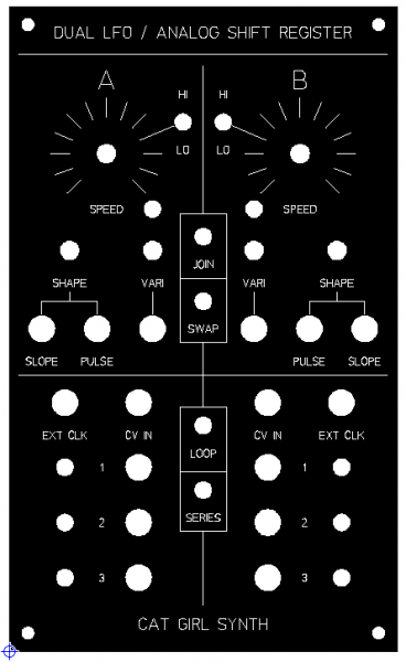
| What are the three holes beside the ASR stages for? LEDs / Switches ? |
|
|
Back to top
|
|
|
inlifeindeath

Joined: Apr 02, 2010
Posts: 316
Location: Albuquerque, NM
|
| Posted: Tue May 22, 2012 1:30 pm Post subject:
|
|
|
so at higher vco frequencies, with a constant voltage at the cv in, i get a noticable "pop" or "click" that goes along with the clock pulses. i'm thinking this might be the 'warble' that ken talks about being a difference in opamp offsets (with the 3140) but I used lf356's so this shouldn't be an issue.
does anyone have any ideas what could be causing this? it's definitely still completely useable, just wondering if this is normal. thanks!
_________________
http://www.youtube.com/user/borisandfef |
|
|
Back to top
|
|
|
kindredlost
Joined: Mar 02, 2011
Posts: 22
Location: usa
|
| Posted: Tue May 22, 2012 4:34 pm Post subject:
|
|
|
| iopop3 wrote: | | What are the three holes beside the ASR stages for? LEDs / Switches ? |
Bypass switches for each stage.
Thanks for the replies. The brighter LED idea sounds good but I hate those blue ones with a passion.
If this module works out the way I'll put up a drawing of the switch logic on the series/loop function. There is interruption of the clock and cv on the "B" register when in series. Everything is done from register "A". The tricky part is the logic between loop with series or loop without series. All clock input jacks are interruptible to break in on the clocks from their adjacent LFO banks. |
|
|
Back to top
|
|
|
andrewF
Joined: Dec 29, 2006
Posts: 1176
Location: australia
Audio files: 4
|
| Posted: Wed May 23, 2012 3:49 am Post subject:
|
|
|
| kindredlost wrote: | The brighter LED idea sounds good but I hate those blue ones with a passion.
|
you can get most colours as superbright now - especially red, they developed them for use in cars |
|
|
Back to top
|
|
|
kindredlost
Joined: Mar 02, 2011
Posts: 22
Location: usa
|
|
|
Back to top
|
|
|
kindredlost
Joined: Mar 02, 2011
Posts: 22
Location: usa
|
|
|
Back to top
|
|
|
zthee

Joined: Feb 20, 2008
Posts: 414
Location: Stockholm
|
| Posted: Tue Jul 03, 2012 4:32 am Post subject:
|
|
|
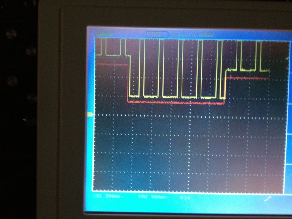
I'd check pin 14 of the 4052 connected to out 1.
Edit - Or check for solderbirdge between pin 15 and pin 16. (Though that would affect the other stages as well.
But since it's cyclical - I.e. every 4th step, something is wrong when it reads from the S&H cell. So my guess would be it's either pin 11, 12, 14 or 15 of the 4052.
_________________
http://www.thehumancomparator.net/ |
|
|
Back to top
|
|
|
kindredlost
Joined: Mar 02, 2011
Posts: 22
Location: usa
|
| Posted: Tue Jul 03, 2012 6:17 pm Post subject:
|
|
|
It is fixed. There was a lifted pad on one of the jumper lines at either pin 11 or 14 of the 4052b chip. zthee gets the prize!
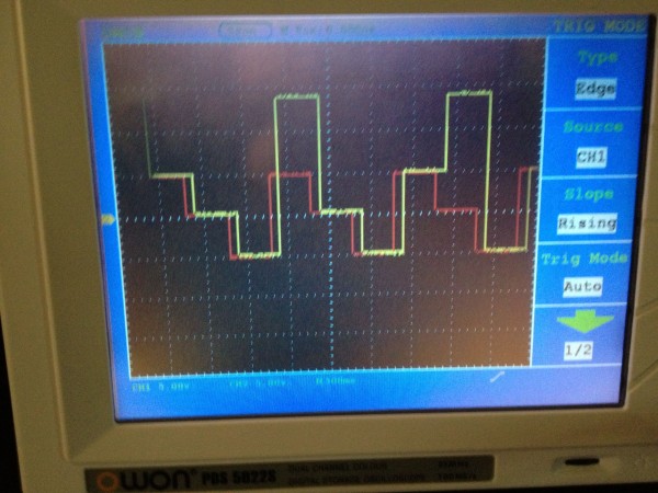
I do have a new question regarding the voltage droop which is (to my knowledge) a common thing on these ASR's. I'm see about 160mv difference in stage 1, 200mv on stage 2 and 220mv on stage three. That much difference from the input voltage (lets say 0 volts). The voltage difference stays the smae regardless of the scale. In other words, if there is 5 volts input then there is 5.16 at stage 1 etc..
I can build a circuit comprised of a 20k resistor and a 4k7 trimmer at the output buffer and the -15v pickup (basically replacing the 22k resistors), but my question is - could building this circuit with .1% resistors (instead of 1%) help to alleviate some of the droop or is it something entirely unrelated?
Thanks for any advise.
-David |
|
|
Back to top
|
|
|
|

 Forum index » DIY Hardware and Software » Ken Stone designs - CGS