| Author |
Message |
heinzer
Joined: Aug 11, 2018
Posts: 12
Location: brooklyn
Audio files: 2
|
 Posted: Wed Nov 10, 2021 10:58 pm Post subject:
DIY 8-BIT SAMPLER - ADVICE NEEDED Posted: Wed Nov 10, 2021 10:58 pm Post subject:
DIY 8-BIT SAMPLER - ADVICE NEEDED |
  |
|
Hey folks - this is going to be my first post/question (though I am a longtime fan and reader of this incredible useful forum)
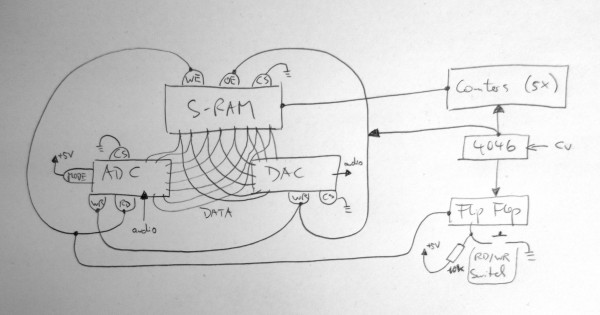
the idea: a simple 8 bit voltage controlled sampler using S-RAM for sample storage…audio/synth signal into ADC -> S-RAM -> DAC - mixer -> audio out…
control mechanisms:
1. voltage controlled clock (4046) timing the counters / ADC / S-RAM / DAC…
2. RD/WR switch using a d-flip flop to align the switch timing with the clock
I got most of the device working…almost 20sec of relatively clean audio looping
the issue: whenever I use the RD/WR switch to insert / record audio, there’s an audible pop in the sample (1x press/start + 1x release/end)…it is only audible in quiet passages, but just too annoying…
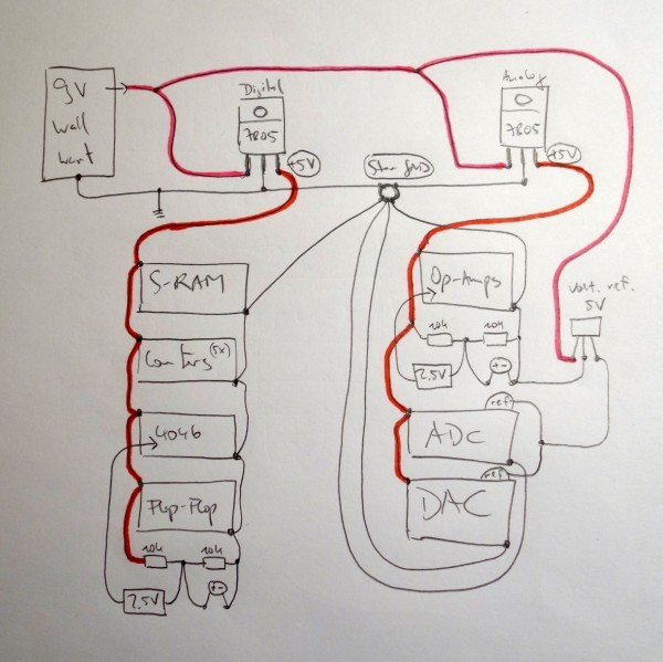
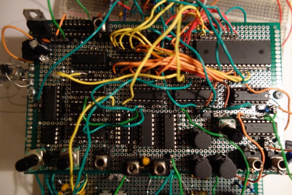
the whole device is build on protoboard (mostly soldered) and has many long overlapping wires between the ICs…see photo…(I assume this could be an issue, but everything else works fine) it runs on 5V provided by a 9V wall wart (high quality) through a voltage regulator (1A)…all the ICs have bypass caps…
I read about timing issues in the nanoseconds between the ICs…I still have to make a timing diagram (was hoping it wouldn’t be necessary)…I first thought the S-RAM is switching the WR ON too early and OFF too late so that the data from the ADC is not valid yet…but there might be something else wrong…
I tried the following:
1. tested ADC audio input while switching -> no pop there (but on the sample)
2. delayed the clock to the S-RAM while keeping the ADC/DAC clock original…(I used different numbers of gates)…still popping, though some gate combinations seem to make it less audible…
3. used jk-flip flop before the RD/WR switch (to avoid grounding the d-flip flop directly)…still popping
4. used NO flip flop to switch RD/WR directly -> still popping
5. took the ADC off…basically no signal into S-RAM…still popping!!! (that is the strangest thing…maybe something related to power source?)
6. I looked at all the logic signals on the oscilloscope…they all have a spike of about +0.6V at the beginning and -0.6V at the end of the square waveform…I tried to filter this out (simple RC filter) -> still popping
any advice would be extremely helpful!!!
the simplified schematics obliterate audio in/out opamps, detailed connections bet counters and S-RAM, voltage control, etc…the 5th counter has 2 unused output pins…should I ground them?
ICs are:
clock - CD4046
ADC - TL0820a
S-RAM - AS6C4008 (512k x 8b)
DAC - TLC7524
Counters (5x) 74HC193
d-flip flop
jk-flip flop
| Description: |
|
| Filesize: |
890.2 KB |
| Viewed: |
151 Time(s) |
| This image has been reduced to fit the page. Click on it to enlarge. |
|
| Description: |
|
| Filesize: |
943.05 KB |
| Viewed: |
158 Time(s) |
| This image has been reduced to fit the page. Click on it to enlarge. |
|
|
|
|
Back to top
|
|
 |
analogmonster

Joined: May 30, 2011
Posts: 93
Location: Germany
|
|
|
Back to top
|
|
|
elektrouwe
Joined: May 27, 2012
Posts: 146
Location: Germany
|
| Posted: Thu Nov 11, 2021 1:44 am Post subject:
Re: DIY 8-BIT SAMPLER - ADVICE NEEDED |
|
|
| heinzer wrote: | ...
5. took the ADC off…basically no signal into S-RAM…still popping!!! (that is the strangest thing…maybe something related to power source?)... |
Do you have a decoupling cap (100n cerco) in every chip socket ?
Did you route seperate digital and analog power lines for 5V and GND ?
Analog GND (DAC,ADC...) connected to digital GND @ a single point ?
Is there a 100uF + 100n were digital and analog power lines connect ? |
|
|
Back to top
|
|
|
blue hell
Site Admin

Joined: Apr 03, 2004
Posts: 24488
Location: The Netherlands, Enschede
Audio files: 298
G2 patch files: 320
|
| Posted: Thu Nov 11, 2021 4:49 am Post subject:
|
|
|
is it plopping also when you record silence?
_________________
Jan
also .. could someone please turn down the thermostat a bit.
 |
|
|
Back to top
|
|
|
Grumble
Joined: Nov 23, 2015
Posts: 1319
Location: Netherlands
Audio files: 30
|
| Posted: Thu Nov 11, 2021 3:32 pm Post subject:
|
|
|
I see you use a multiplying DAC, is the Vref stable?
_________________
my synth |
|
|
Back to top
|
|
|
heinzer
Joined: Aug 11, 2018
Posts: 12
Location: brooklyn
Audio files: 2
|
|
|
Back to top
|
|
|
elektrouwe
Joined: May 27, 2012
Posts: 146
Location: Germany
|
| Posted: Fri Nov 12, 2021 2:23 am Post subject:
|
|
|
| heinzer wrote: | ...
electrouwe: I was not aware of having to separate the digital (logic) and analog (opamps, etc) power/GND lines... |
google for "star ground" and you will find lots of information, why separate GNDs and VCCs are important and how to do it.
Your RAM will probably draw >100mA spikes when switching modes/access.
If these fast current spikes turn into voltage when flowing through a inductance ( which your GND wiring is) , you will have it everywhere on your board. So please take your time and do the right power line routing.
And yes, opamp GND must be analog GND. |
|
|
Back to top
|
|
|
heinzer
Joined: Aug 11, 2018
Posts: 12
Location: brooklyn
Audio files: 2
|
| Posted: Sat Nov 13, 2021 8:53 pm Post subject:
|
|
|
thx electrouwe for the "star ground" idea...I did a lot of reading on this but still have a few questions (pros/cons of star ground vs. separate ground planes)
1. ADC/DAC are considered analogue, right?
2. the voltage reference for the 4046 should connect to digital ground, right? do you suggest using a voltage reference IC too? (instead of a simple voltage divider)
3. a star ground would implement routing EVERY ground connection to a central point? OR combining all analogue and all digital grounds and then letting those meet at a central point (isn't this like having 2 ground planes?)
4. what about the power lines? they should just be linked separately (1x combined analogue / 1x combined digital) right?
5. some designers even suggested having 2 separate power supplies for analgogue / digital (1 voltage converter for each?) like dividing the power input (9V) to 2 voltage converters (and then having basically 2 grounds)?
any advice would be highly appreciated....thx |
|
|
Back to top
|
|
|
elektrouwe
Joined: May 27, 2012
Posts: 146
Location: Germany
|
| Posted: Sun Nov 14, 2021 5:16 am Post subject:
|
|
|
| heinzer wrote: | | 1. ADC/DAC are considered analogue, right? |
yes. But because both are also digital and produce current glitches on GND, I would route them separatly to the star GND point to avoid coupling this noise into other analog parts
| heinzer wrote: | | 2. the voltage reference for the 4046 should connect to digital ground, right? do you suggest using a voltage reference IC too? |
need detailed schematics to answer more specific.
| heinzer wrote: | | 3. a star ground would implement routing EVERY ground connection to a central point? |
that would be an overkill - we talk about 8bit electronics. I guess you can use serial VCC and DGND wiring for the digital glue logic, which is then routed to the star ground point with a single wire. Same applies for analog "reference" GND, like noninverting opamp inputs. If analog components don't draw excessive current , which would cause DC offset voltages on GND or they don't produce switching noise, I would route them from point to point and then route this AGND to star ground.
| heinzer wrote: | | 4. what about the power lines? they should just be linked separately |
Loops in general should be avoided, which means that VCC and GND nets should be routed as close as possible minimize the loop area.
I would try to "copy" the DGND wiring topology also for VSS, and also route analog VSS close to AGND wires.
| heinzer wrote: | | 5. some designers even suggested having 2 separate power supplies for analgogue / digital (1 voltage converter for each?) like dividing the power input (9V) to 2 voltage converters (and then having basically 2 grounds)? |
I would consider 2 power supplies, or do extra LC filtering for critical parts with single supply, for a 12 or 16bit design. But it woulde be easy to add a 2nd voltage regulator later , because you should have separate analog and digital VCC routing anyway |
|
|
Back to top
|
|
|
heinzer
Joined: Aug 11, 2018
Posts: 12
Location: brooklyn
Audio files: 2
|
|
|
Back to top
|
|
|
elektrouwe
Joined: May 27, 2012
Posts: 146
Location: Germany
|
| Posted: Tue Nov 16, 2021 2:23 am Post subject:
|
|
|
| heinzer wrote: |
1. ADC/DAC: do you recommend routing the VCC separately too? |
give it a try, soldering 1 wire takes less time than our discussion 
You will gain design experience if you check out different ideas. Take advantage of having a breadboard and not a PCB !
| heinzer wrote: | | 2. the "voltage reference" is a little IC looking like a transistor...I use it for the reference voltage (5V) for the ADC/DAC |
I doubt that you need a TL431 or similar for an 8 bit audio design. We talk about 5V/256 = 20mV/bit. Your analog 7805 should have much less than 20mV noise, so it should be fine. 5V temperature drift is also not an issue here, because long time drifts will appear as inaudible "milli dB" amplitude drifts.
Same for the 4046 reference: good filtering keeps VCO Jitter low, but there is no need for high absolute precision
| heinzer wrote: | | 5. is it making sense to use 2x +5V voltage converters (to separate digital from analog)? see picture (can you check if the routing makes sense? I intentionally left out all the caps) |
see 1. 
| heinzer wrote: | | new question: should I also route the S-RAM separately, since it seems to be the source of the popping issue |
I would do it; but again - see 1.
now warm up your solder iron and tell us about your findings ! |
|
|
Back to top
|
|
|
heinzer
Joined: Aug 11, 2018
Posts: 12
Location: brooklyn
Audio files: 2
|
| Posted: Wed Nov 17, 2021 10:57 pm Post subject:
|
|
|
thx again...irons will be warmed up shortly... 
will share my findings soon!!! (probably in a couple of weeks) |
|
|
Back to top
|
|
|
der Warst

Joined: Apr 09, 2010
Posts: 10
Location: Leipzig
|
| Posted: Sun Oct 05, 2025 6:36 am Post subject:
|
|
|
Hey, sorry for digging this up, but I'm more or less building the same thing right now (my schematic is ~90% the same as yours), and I was wondering: Did you ever figure out your popping problem? Also, what became of the project in general?
Also, thanks for the useful info here. It's probably gonna come in handy once I've built my version.
_________________
http://www.warstware.der-warst.de |
|
|
Back to top
|
|
|
|

 Forum index » DIY Hardware and Software