| Author |
Message |
spookyandwhatnot
Joined: Dec 19, 2017
Posts: 2
Location: somewhere
|
|
|
Back to top
|
|
 |
PHOBoS
Joined: Jan 14, 2010
Posts: 5794
Location: Moon Base
Audio files: 709
|
 Posted: Tue Dec 19, 2017 11:30 am Post subject: Posted: Tue Dec 19, 2017 11:30 am Post subject:
|
  |
|
 
I could do a whole write up about cmos chips and there are some guides floating around on this forum but I think
this page should get you started.
some basic info:
Never leave any inputs floating (unconnected) this also important if you don't use all the gates in one chip. Unused inputs
are often connected to GND but you could connect them to the positive rail as well, it depends a bit on their function.
Also connect small decoupling capacitors (100nF is pretty standard) close to the power input pin of every chip (often pin 14 or 16)
and GND. To understand how the chips function and how to connect them datasheet are really useful but can be a bit hard
to get into if you're a novice.
I don't know how much experience you have and what you know about electronics in general but I advice you to experiment
using a breadboard to get some understanding of how things function. Lunettas are a great introduction for getting to know
the basics. If you don't understand something, just ask. There are a lot of helpful people here especially in this section of the forum.
have fun on your journey 
_________________
"My perf, it's full of holes!"
http://phobos.000space.com/
SoundCloud BandCamp MixCloud Stickney Synthyards Captain Collider Twitch YouTube |
|
|
Back to top
|
|
|
Steveg

Joined: Apr 23, 2015
Posts: 184
Location: Perth, Australia
|
| Posted: Wed Dec 20, 2017 5:33 am Post subject:
|
|
|
hi Spookyandwhatnot,
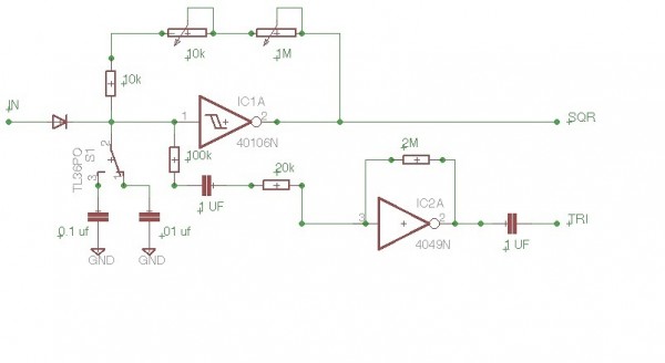
You'll see on the diagram two weird shapes labelled IC1A and IC2A. They are the integrated circuit logic components. So IC = Integrated Circuit 1 or 2 is the chip number 1 is the first chip 2 is the second and so on. The last letter is the circuit within the chip so A is the first circuit, B the second and so on. Now you can look up the data sheet for a CD40106 and find the pin numbers for each circuit but you can see on the circuit diagram there are numbers near the left and right sides of the symbol so IC1A uses pins 1&2 and IC2A uses pins 2&3 (on a different chip). You will need to consult the datasheet to find out where the chip's power (VCC) and earth (VSS) are located. Also to locate any unused inputs for other chip circuits and follow Phobos' recommendations.
Enjoy!
Steveg |
|
|
Back to top
|
|
|
stolenfat

Joined: Apr 17, 2008
Posts: 476
Location: Sunny Oakland California
Audio files: 1
|
| Posted: Sun Dec 24, 2017 8:47 pm Post subject:
|
|
|
Since your new (welcome) I recommend you research the slacker melody generator after this. It's a 2 chip circuit based off very cheap cmos ics... it's a little troubling to perf for a beginner BUT it can connect directly to a 40106 (SQR wave) clock bank and you get some amazing fun results.
I recommend it for a few reasons.
1. knowledge of "modular" connectivity - deciding what kind of connectors your into, signal flow
2. knowledge of cmos basics - grounding unused gates, 100k pull down resistors, ect
3. Perf/soldering skills
4. Builds up your collection of components
5. easy to troubleshoot
essentially it makes a great building block for future circuits and i'd say my explorations with that 1 particular circuit really opened my eyes. I don't use it too much now-a-days now that i've honed in on my personal tastes but the amount I learned from that circuit was great. Really fun hands on way of making something cool if you learn that way.
Here's a link to the schematic and there's tons of info on it at electromusic.
Edit: forgot to post the link.
http://www.electro-music.com/forum/topic-42552.html
_________________
home made noise and electronic ill-logic |
|
|
Back to top
|
|
|
|

 Forum index » DIY Hardware and Software » Lunettas - circuits inspired by Stanley Lunetta