| Author |
Message |
kxspxr

Joined: Nov 20, 2008
Posts: 35
Location: Denmark
|
|
|
Back to top
|
|
 |
DrJustice

Joined: Sep 13, 2004
Posts: 2114
Location: Morokulien
Audio files: 4
|
 Posted: Thu Nov 20, 2008 12:19 pm Post subject: Posted: Thu Nov 20, 2008 12:19 pm Post subject:
|
  |
|
Hi kxspxr!
 to electro-music.com! to electro-music.com!
| Quote: | | I have stared myself blind and I can't seem to find the error. |
We've all been there...
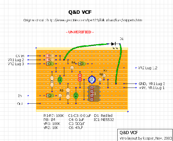
I haven't gone through everything - the schematic has no component or pin numbers, which makes it a bit tedious to relate to the vero. Perhaps you have a schematic that is numbered like the vero?
However, the first things I see is that VR2 lugs 1,2 are connected to R3, R4 and C5, i.e. it's connected to one more resistor than shown in the schematic. And, R4 seems to be shorted out by the link 4 holes to the left of it.
DJ
-- |
|
|
Back to top
|
|
|
kxspxr
Joined: Nov 20, 2008
Posts: 35
Location: Denmark
|
| Posted: Thu Nov 20, 2008 1:11 pm Post subject:
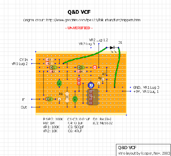
VCF vero layout |
|
|
Thanks for the reply! - I have been lurking the forums for a while, though.
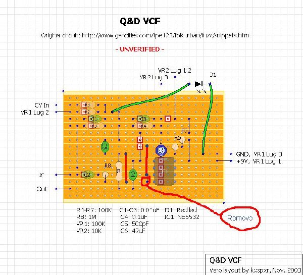
Arggh! Why didn't I see that? R4 is shorted on the layput but not on my "real" board. Sorry about that. I have modified the layout a bit and decided to resolder the whole thing.
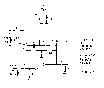
Before I do that, perhaps somone will have a look at the layout? I included the schematic with matching component numbers.
| Description: |
|
| Filesize: |
3.19 KB |
| Viewed: |
13893 Time(s) |
|
| Description: |
|
| Filesize: |
24.85 KB |
| Viewed: |
363 Time(s) |
| This image has been reduced to fit the page. Click on it to enlarge. |
|
_________________
"Posthumanity is a discrete set of processes with arbitrary return codes." |
|
|
Back to top
|
|
|
DrJustice
Joined: Sep 13, 2004
Posts: 2114
Location: Morokulien
Audio files: 4
|
|
|
Back to top
|
|
|
kxspxr
Joined: Nov 20, 2008
Posts: 35
Location: Denmark
|
| Posted: Thu Nov 20, 2008 2:18 pm Post subject:
VCF vero layout |
|
|
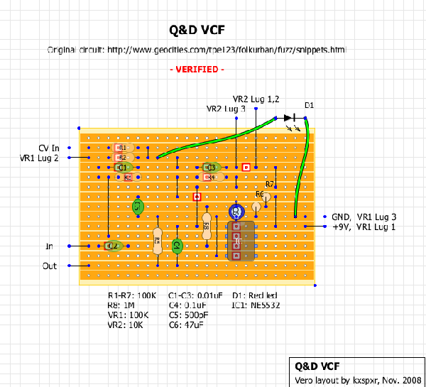
Thanks a bunch! I thought the bias was supposed to connect to GND of the chip (pin 4), making it a virtual ground. But it makes pretty good sense that it should connect to the + input of the opamp (pin 3). The headroom will be greater if I power it with two 9V batteries and omit the voltage divider section on the powersupply, right? I'm still learning..
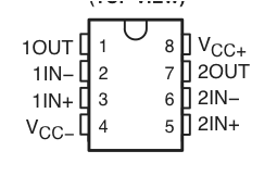
Sorry, forgot to include 5532 pinout -here it is along with a corrected layout. Again, thanks a lot for your help! It all makes perfect sense now.
| Description: |
|
| Filesize: |
8.2 KB |
| Viewed: |
13884 Time(s) |
|
| Description: |
|
| Filesize: |
17.74 KB |
| Viewed: |
376 Time(s) |
| This image has been reduced to fit the page. Click on it to enlarge. |

|
_________________
"Posthumanity is a discrete set of processes with arbitrary return codes." |
|
|
Back to top
|
|
|
DrJustice
Joined: Sep 13, 2004
Posts: 2114
Location: Morokulien
Audio files: 4
|
| Posted: Thu Nov 20, 2008 5:23 pm Post subject:
Re: VCF vero layout |
|
|
| kxspxr wrote: | | The headroom will be greater if I power it with two 9V batteries and omit the voltage divider section on the powersupply, right? |
That's right! Taking GND and the bias voltage from between the two 9V batteries. You still need the current limiting series resistor on the bias voltage. So, using a dual rail power supply we'd get :
| Code: |
+------ +V (to NE5532 Vcc+ and VR1 lug 1)
|
---
- +--[R8]-- bias voltage to NE5532 1in+
| |
+---+-- GND
|
---
-
|
+------ -V (to NE5532 Vcc-)
|
There's lots of fun little circuits on that link in your first posting - DIY'ers take notice. Let us know how it sounds when you have it working then 
DJ
-- |
|
|
Back to top
|
|
|
kxspxr
Joined: Nov 20, 2008
Posts: 35
Location: Denmark
|
| Posted: Fri Nov 21, 2008 2:53 am Post subject:
|
|
|
I am just about to solder it from the corrected design. As far as I can see, R8 should not connect to ground but instead to half the supply voltage instead. Connecting it to ground as shown on the layout makes a hipass with a cutoff of 100hz on the input. I don't want that, so I will omit the jumper from bias to pin 3 and connect R8 there instead. That would be right according to the schematic, right? As far as I understand, connecting R8 to the bias will give a current of 4.5uA on pin 3, provided a 9v power supply. My questions are (if I understand this correct) why do I need R8 and how do I choose an appropriate value for it?
I'll post my results as soon as I have them.
_________________
"Posthumanity is a discrete set of processes with arbitrary return codes." |
|
|
Back to top
|
|
|
kxspxr
Joined: Nov 20, 2008
Posts: 35
Location: Denmark
|
|
|
Back to top
|
|
|
richardc64

Joined: Jun 01, 2006
Posts: 679
Location: NYC
Audio files: 26
|
|
|
Back to top
|
|
|
kxspxr
Joined: Nov 20, 2008
Posts: 35
Location: Denmark
|
| Posted: Fri Nov 21, 2008 5:56 am Post subject:
|
|
|
| richardc64 wrote: |
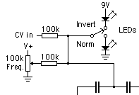
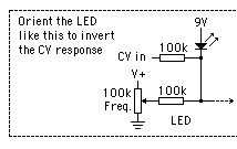
The led isn't meant to be a visual indicator. It's used for its conductive properties, and so can be mounted on the board. You could add a 2nd led to +9v as shown in the original schematic and an spdt switch to change the response from up sweep to down. |
Wouldn't I need a resistor between +9V and the led to avoid destroying it?
_________________
"Posthumanity is a discrete set of processes with arbitrary return codes." |
|
|
Back to top
|
|
|
DrJustice
Joined: Sep 13, 2004
Posts: 2114
Location: Morokulien
Audio files: 4
|
| Posted: Fri Nov 21, 2008 6:17 am Post subject:
|
|
|
| kxspxr wrote: | As far as I can see, R8 should not connect to ground but instead to half the supply voltage instead.
|
Ah, yes! I forgot that, but you caught it so now you're in control 
| Quote: | It works and is sounds quite neat. I only tried feeding it with a square wave. It's well worth the effort. I have updated the layout. This is the *right* one
|
Great - There's nothing like rolling your own!
| Quote: |
The led doesn't light up when I turn VR1. It doesn't seem to affect the overall performance of the circuit, however. I suppose it's because of R2. |
Yes. With VR1 at the fully positive position, R1 and R2 will be in parallel and their total resistance is:
1/(1/R1+1/R2) = 50000ohm
so the maximum current through the LED is limited to :
9/50000 = 0.18mA
That's not enough current for the LED to produce much light.
However, the LEDs function in this circuit is not to produce light, but to limit the range of the frequency controlling voltage. A typical LED has a forward voltage drop of ca. 2V (varies with colour and type). That results in the voltage at the node where R1,R2,LED,C1,C2 meets always being at least 2V above ground. What you get from adjusting VR1 is a variable current source. (Please correct me someone, if I'm wrong!)
Edit: Aha! I see richardc64 was quicker than me 
Edit2: typo
Edit3: typo again 
DJ
--
Last edited by DrJustice on Fri Nov 21, 2008 6:30 am; edited 3 times in total |
|
|
Back to top
|
|
|
richardc64
Joined: Jun 01, 2006
Posts: 679
Location: NYC
Audio files: 26
|
|
|
Back to top
|
|
|
kxspxr
Joined: Nov 20, 2008
Posts: 35
Location: Denmark
|
| Posted: Fri Nov 21, 2008 8:27 am Post subject:
|
|
|
| DrJustice wrote: | However, the LEDs function in this circuit is not to produce light, but to limit the range of the frequency controlling voltage.
-- |
It makes perfect sense now. Thanks for the thorough explanation. I'll install a switch as richardc64 suggested and begin working on a 4017 modular cv sequencer - I want to hook it up to the filter
_________________
"Posthumanity is a discrete set of processes with arbitrary return codes." |
|
|
Back to top
|
|
|
|

 Forum index » DIY Hardware and Software » Developers' Corner