| Author |
Message |
crazeydazey

Joined: Feb 15, 2007
Posts: 303
Location: England
Audio files: 4
|
|
|
Back to top
|
|
 |
numbernone
Joined: Aug 16, 2006
Posts: 477
Location: new york city
|
 Posted: Wed Jan 30, 2008 8:27 am Post subject: Posted: Wed Jan 30, 2008 8:27 am Post subject:
|
  |
|
I will be watching, as I am also in the throes of learning Eagle. IT AINT EASY. I think I also downloaded the same library, not much in it, except it did have the 2SA798, for which I had the pinouts wrong!
I wish I had your answer... |
|
|
Back to top
|
|
|
Sebo

Joined: Apr 27, 2007
Posts: 564
Location: Argentina
|
| Posted: Wed Jan 30, 2008 8:47 am Post subject:
|
|
|
Hi:
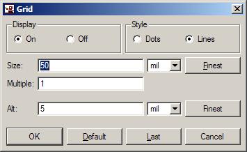
Check the grid settings, or disable it. I think that's could be the problem.
Where do you downlad sdiy library from?
_________________
Sebo
---------------------------------------
My Music:
https://www.facebook.com/cosaquitos/ |
|
|
Back to top
|
|
|
crazeydazey
Joined: Feb 15, 2007
Posts: 303
Location: England
Audio files: 4
|
|
|
Back to top
|
|
|
bugbrand

Joined: Nov 27, 2005
Posts: 846
Location: Bristol, UK
Audio files: 1
G2 patch files: 1
|
| Posted: Wed Jan 30, 2008 11:56 am Post subject:
|
|
|
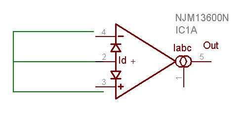
Ahhh, I found exactly the same problem when I started using the SynthDIY library! Many of the packages are on a funny grid (maybe mm rather than inch)
I like to keep the schematic on a standard grid (0.1") so I edited the library::
- Go to the control panel and expand the Libraries view
- scroll to the SynthDIY Library, right click it and select Open
- near the top left of the tool bars you'll see three little symbols for Device, Package and Symbol. First click the Device one and find the part you want to edit.
- select the Info tool (topish left) and find out what Symbol is being used for the device - with the NJM13600 (and LM13700 etc) you'll find that the main opamp part uses the Symbol OTA_WD_N . Also check what the buffer Symbol is (..OTA_BUF)
- right, now click the Symbol button on the toolbar and hunt out the OTA_WD_N symbol. This is the bit you edit, moving the pins around so that they're on your favourite grid -- I do this by switching between different grids and cross comparing until I've moved everything onto the 0.1" grid.
- do the same for OTA_BUF
- these changes will automatically be updated to the Devices that use that Symbol within the library (you can check back to the Device NJM13600 to see). Now save your changes, close the library and head back to the schematic.
- If you've already got your NJMs included in the schematic you'll need to update them - go to the top and open the Library menu and click Update All.
Hope that is just about understandable! Took me ages to discover how to clunk around with the libraries... But its definitely worth a poke in the long run.
_________________
http://www.bugbrand.co.uk
http://www.bugbrand.blogspot.com |
|
|
Back to top
|
|
|
Clack

Joined: Aug 08, 2005
Posts: 438
Location: Walthamstow - london
Audio files: 5
G2 patch files: 1
|
| Posted: Wed Jan 30, 2008 2:54 pm Post subject:
|
|
|
its on a 0.635mm grid ( 0.025" ) which is pretty fine
_________________
Clacktronics.co.uk |
|
|
Back to top
|
|
|
crazeydazey
Joined: Feb 15, 2007
Posts: 303
Location: England
Audio files: 4
|
| Posted: Thu Jan 31, 2008 2:22 am Post subject:
|
|
|
Cheers guys..
I've had a play with the library, just to learn how to create my own components and stuff, which is fun. but I'm quite happy to change the grid size for now.
One thing I did do with the LM13600N was turn pin 1 so it's pointing up, as that's how it is on the circuit I'm copying, so I guess that was a good learning experience.
what I'm doing is putting some of the circuit diagrams I've found (MFOS, EFM etc) into Eagle so I can 1, learn Eagle and 2, create my own PCBs from them.. I hope this isn't infringing copyright laws or anything.. they are for my personal use, I have no intention of selling them or anything..
it's just that ray is quite happy to give you circuit diagrams and PCB layouts where tom only provides circuit diagrams..
so if creating my own PCBs (for personal use) from other peoples schems is naughty, let me know and I'll stop. |
|
|
Back to top
|
|
|
Clack
Joined: Aug 08, 2005
Posts: 438
Location: Walthamstow - london
Audio files: 5
G2 patch files: 1
|
| Posted: Thu Jan 31, 2008 2:50 am Post subject:
|
|
|
Not at all, its your own artwork. Its even fine if you release the PCB into public - If you start selling them even then its a bit fuzzy and probably perfectly fine ( well fine as in you probably wont get sued ) as you made the image - you should look at the thread in this forum about it. I think the conclusion is, that its just all about being nice and not undercutting people who give things away for free.
_________________
Clacktronics.co.uk |
|
|
Back to top
|
|
|
crazeydazey
Joined: Feb 15, 2007
Posts: 303
Location: England
Audio files: 4
|
| Posted: Thu Jan 31, 2008 3:02 am Post subject:
|
|
|
 cool.. cool..
I'm not into this to make any money out of it, but if I do anything of any use to anyone I will post it here... |
|
|
Back to top
|
|
|
loss1234

Joined: Jul 24, 2007
Posts: 1536
Location: nyc
Audio files: 41
|
|
|
Back to top
|
|
|
crazeydazey
Joined: Feb 15, 2007
Posts: 303
Location: England
Audio files: 4
|
| Posted: Thu Jan 31, 2008 7:23 am Post subject:
|
|
|
I wish you could that would be cool..
Unfortunately I'm redrawing the circuit diagrams in eagle, and building the PCB designs from there..
I'm just working on rene's 4069 VCO at the moment |
|
|
Back to top
|
|
|
crazeydazey
Joined: Feb 15, 2007
Posts: 303
Location: England
Audio files: 4
|
|
|
Back to top
|
|
|
etaoin

Joined: Jun 30, 2005
Posts: 761
Location: Utrecht, NL
|
| Posted: Fri Feb 01, 2008 8:00 am Post subject:
|
|
|
| crazeydazey wrote: | | please have a look and let me know what you think.. |
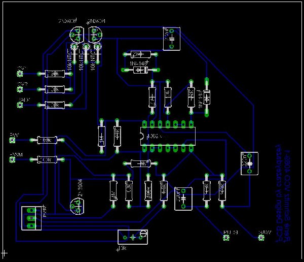
You seem to be missing power decoupling, for one.
Was this done with the autorouter? There are some odd routing decisions, especially around the power connector. I would never put traces through that myself, but what do I know.
I'd also opt for slightly wider traces especially if you're going to etch this yourself. Filling up the empty space will also save you a lot of etching fluids.
_________________
http://www.casia.org/modular/ |
|
|
Back to top
|
|
|
crazeydazey
Joined: Feb 15, 2007
Posts: 303
Location: England
Audio files: 4
|
| Posted: Fri Feb 01, 2008 8:10 am Post subject:
|
|
|
I guess I could put decoupling on, I just copied it from http://www.uni-bonn.de/~uzs159/index.html. I've also realised I haven't put anyware to attach gnd etc to pots and jacks.
Also I've just noticed there is no gate on this VCO.. How do you trigger it??
I was going to make it as a simple VCO but I've confused myself now..
yeah I used the autorouter, I'm not clever enough to do the routing myself just yet.. still a noob.  |
|
|
Back to top
|
|
|
etaoin
Joined: Jun 30, 2005
Posts: 761
Location: Utrecht, NL
|
| Posted: Fri Feb 01, 2008 8:12 am Post subject:
|
|
|
| crazeydazey wrote: | | Also I've just noticed there is no gate on this VCO.. How do you trigger it?? |
It's a VCO. A VCO doesn't have a gate.
_________________
http://www.casia.org/modular/ |
|
|
Back to top
|
|
|
crazeydazey
Joined: Feb 15, 2007
Posts: 303
Location: England
Audio files: 4
|
| Posted: Fri Feb 01, 2008 8:17 am Post subject:
|
|
|
 of course it doesn't what the hell am I talking about???? of course it doesn't what the hell am I talking about????
I told you I'd confused myself. |
|
|
Back to top
|
|
|
loss1234
Joined: Jul 24, 2007
Posts: 1536
Location: nyc
Audio files: 41
|
|
|
Back to top
|
|
|
Clack
Joined: Aug 08, 2005
Posts: 438
Location: Walthamstow - london
Audio files: 5
G2 patch files: 1
|
| Posted: Sat Feb 02, 2008 4:12 am Post subject:
|
|
|
electronic peasant has a good intro on decoupling
http://www.electronicpeasant.com/circuits/decouple.txt
Always put it in first - it saves a lot of hassle - people like rene may not put it in the schematic as its assumed you know to do it. I recommended to breadboard things first , many things don't work straight from the scematic
I would also reccomend using larger tracks and pads - eagles defaults are incredibly small for press and peel - a 0.8 drill will almost obliterate all the copper in a small pad. Another thing is that thinner tracks tend to be more fragile - if you have a transistor say , and your a bit rough with it after soldering it in - it will probably rip up the tracks if too thin ( this is if your using cheapo PCB boards like me though )
You also have to think about how close pads are to the tracks as solder tends to jump to across as there isn't a soldermask. if you run 2 tracks too close to each other for long enough they will probably interfere - i try to keep things 2-3 mil apart
Another thing you'll probably come across soon is analogue ground and digital ground in schematics - here is a little post that helped me understand
http://www.epanorama.net/wwwboard/messages/16215.html
I also think ( this is my preference ) that it is better to put in a jumper wire than make a board 1cm wider or taller . you can do this whilst drawing a bottom layer track select top layer at the top of the screen draw the top layer then press bottom layer and draw it to the destination it will automatically add pads.
A good idea is to set the power up before anything else, some people like to line all the chips up and then put the power lines down the centre of them all - then put decoupling caps for each chip inbetween
hope that helps
_________________
Clacktronics.co.uk |
|
|
Back to top
|
|
|
crazeydazey
Joined: Feb 15, 2007
Posts: 303
Location: England
Audio files: 4
|
|
|
Back to top
|
|
|
crazeydazey
Joined: Feb 15, 2007
Posts: 303
Location: England
Audio files: 4
|
| Posted: Fri Feb 15, 2008 5:41 am Post subject:
|
|
|
did anyone ever do anything with the ZIP file I attached??
I'd be interested to see what other people come up with.. |
|
|
Back to top
|
|
|
Sebo
Joined: Apr 27, 2007
Posts: 564
Location: Argentina
|
| Posted: Fri Feb 15, 2008 7:06 am Post subject:
|
|
|
Hi:
I downloaded the file, but I didn't have the time to open it.
I will build a 4069 in the future, so, in some point I will open it.
Thanks for sharing.
_________________
Sebo
---------------------------------------
My Music:
https://www.facebook.com/cosaquitos/ |
|
|
Back to top
|
|
|
crazeydazey
Joined: Feb 15, 2007
Posts: 303
Location: England
Audio files: 4
|
| Posted: Fri Feb 15, 2008 7:25 am Post subject:
|
|
|
cool
I'm a noob with a lot to learn so I would love to see other peoples work around this... |
|
|
Back to top
|
|
|
etaoin
Joined: Jun 30, 2005
Posts: 761
Location: Utrecht, NL
|
| Posted: Fri Feb 15, 2008 7:42 am Post subject:
|
|
|
| crazeydazey wrote: | | I'm a noob with a lot to learn so I would love to see other peoples work around this... |
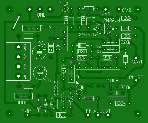
This is what I was working on earlier. It is still unchecked and there's a nasty wire I needed to connect the ground plane, which I still want to get rid of.
| Description: |
| 4069 VCO preliminary PCB design |
|
| Filesize: |
158.39 KB |
| Viewed: |
8262 Time(s) |
|
| Description: |
| 4069 VCO prelim PCB design PDF |
|

Download (listen) |
| Filename: |
4069vco.pdf |
| Filesize: |
26.4 KB |
| Downloaded: |
205 Time(s) |
_________________
http://www.casia.org/modular/
Last edited by etaoin on Fri Feb 15, 2008 8:42 am; edited 5 times in total |
|
|
Back to top
|
|
|
crazeydazey
Joined: Feb 15, 2007
Posts: 303
Location: England
Audio files: 4
|
| Posted: Fri Feb 15, 2008 8:18 am Post subject:
|
|
|
luv it..
if you check it and it's fine, I think this is the beauty I'm gonna try building.
I'll get some Print and peel and some etching stuff... (this will be a first too, I've not tried making my own PCBs yet.) |
|
|
Back to top
|
|
|
Sound
Joined: Jun 06, 2006
Posts: 842
Audio files: 1
|
| Posted: Mon Mar 24, 2008 6:23 am Post subject:
|
|
|
| bugbrand wrote: | Ahhh, I found exactly the same problem when I started using the SynthDIY library! Many of the packages are on a funny grid (maybe mm rather than inch)
I like to keep the schematic on a standard grid (0.1") so I edited the library::
- Go to the control panel and expand the Libraries view
- scroll to the SynthDIY Library, right click it and select Open
- near the top left of the tool bars you'll see three little symbols for Device, Package and Symbol. First click the Device one and find the part you want to edit.
- select the Info tool (topish left) and find out what Symbol is being used for the device - with the NJM13600 (and LM13700 etc) you'll find that the main opamp part uses the Symbol OTA_WD_N . Also check what the buffer Symbol is (..OTA_BUF)
- right, now click the Symbol button on the toolbar and hunt out the OTA_WD_N symbol. This is the bit you edit, moving the pins around so that they're on your favourite grid -- I do this by switching between different grids and cross comparing until I've moved everything onto the 0.1" grid.
|
Hello bugbrand I achieved arrive to this point but I don't achieve to edit the symbol. I try to move the pins but it not coincide with the grid.
What I'm doing wrong? |
|
|
Back to top
|
|
|
|

 Forum index » DIY Hardware and Software