| Author |
Message |
gmeredith
Joined: Jun 28, 2006
Posts: 82
Location: Tasmania, Australia
Audio files: 1
|
 Posted: Wed Jul 12, 2006 8:17 pm Post subject:
Non-volatile memory expansions - how to? Posted: Wed Jul 12, 2006 8:17 pm Post subject:
Non-volatile memory expansions - how to? |
  |
|
Does anyone know how to expand the RAM memory of something with SRAM memory? People have done it. Here is a guy who has been doing memory expansions on Roland Basslines for years:
http://www.firstpr.com.au/rwi/dfish/memory/
He also does it to other types of instruments.
I'd like to do a similar expansion to my Casio sk8 sampling keyboard.
Does anyone know the basics behind doing these sorts of mods?
cheers, Graham |
|
|
Back to top
|
|
 |
mi_dach

Joined: Dec 17, 2005
Posts: 133
Location: Sweden
|
| Posted: Sun Jul 16, 2006 1:35 am Post subject:
Re: Non-volatile memory expansions - how to? |
|
|
| gmeredith wrote: | Does anyone know how to expand the RAM memory of something with SRAM memory? People have done it. Here is a guy who has been doing memory expansions on Roland Basslines for years:
http://www.firstpr.com.au/rwi/dfish/memory/
He also does it to other types of instruments.
I'd like to do a similar expansion to my Casio sk8 sampling keyboard.
Does anyone know the basics behind doing these sorts of mods?
cheers, Graham |
Probably (but I don't know for certain) you can cut the data and address lines running to the machines original RAM. You take another RAM chip (with lots more ram in it) and connect up the data lines. You connect up the existing address bus as the lower end of the address, and you install a bunch of switches that'll toggle the higher bits of the address between 1 and 0. This will give the result described.
Not all RAM chips are equal, so you might need to eperiment with a few diferent sorts, but I'm guessing that basically it's not much more complicated than above. The hard part is probably figuring out where the data and address bus are. Lots of RAM chips are are cheap and uncomplicated.
If you've any more questions, feel free ! Good luck  |
|
|
Back to top
|
|
|
gmeredith
Joined: Jun 28, 2006
Posts: 82
Location: Tasmania, Australia
Audio files: 1
|
| Posted: Sun Jul 16, 2006 4:57 pm Post subject:
|
|
|
After searching, this chip apparently seems to be the direct replacement for the SK8 chip, except better, because it retains its memory without power (has an inbuilt Li-ion battery). So if the batteries in my SK8 go flat, I still won't lose the samples!
DS1230Y NVRAM
http://www.jameco.com/webapp/wcs/stores/servlet/ProductDisplay?langId=-1&storeId=10001&catalogId=10001&productId=114323
Looking at the datasheets (see attachments below), the DS1230Y NVRAM appears to be fairly much pin for pin the same as the original SK8 RAM (uPD2168C-20).
If I stacked one of these on top of the original RAM, which pin(s) would I put a toggle switch on, in order to select between the 2 sets of RAMs?
Cheers, Graham
| Description: |
|

Download (listen) |
| Filename: |
DS1230Y NVRAM.pdf |
| Filesize: |
504.46 KB |
| Downloaded: |
535 Time(s) |
| Description: |
|
Download (listen) |
| Filename: |
uPD4168-20 RAM.pdf |
| Filesize: |
669.37 KB |
| Downloaded: |
603 Time(s) |
|
|
|
Back to top
|
|
|
mi_dach
Joined: Dec 17, 2005
Posts: 133
Location: Sweden
|
| Posted: Mon Jul 17, 2006 1:15 am Post subject:
|
|
|
| gmeredith wrote: | If I stacked one of these on top of the original RAM, which pin(s) would I put a toggle switch on, in order to select between the 2 sets of RAMs?
|
Sadly, stacking them is not an option. You need to remove the original chip, and replace it with this new one that you've found. I don't see why you would want to keep the original chip in place anyway, the newer ram going in will store everything in a similar way, and (hopefully) the original machine wont actually notice whats going on. (It's a little unclear what'll happen when you switch banks, it'd be best to do this when the memory is not being accessed, probably when theres nothing playing. If the ram is in use when you change banks, it might still work, it also might emit garbage or crash. Do let us know!)
Before you start working on this, let me save my ass with a disclaimer. Please, please don't blame me if you damage or destroy anything. I _think_ this works but since I don't have the parts, and haven't studied the datasheets as much as I should... well, at your own risk ok ?
Unsoldering the original ram chip can be tricky if you haven't tried this before, you'll need a solder pump or some of that copper weave thread to suck up the solder, and do practice on some junk first. It'll get hot, so pause every so often to avoid overheating.
Once you get the ram out, install a socket in it's place. You should be able to pop the original chip back in through this in case the new ram doesn't work...
Place the new ram into a second socket. You need to make the following adjustments to the socket itself. The Refresh and CS legs shouldn't connect to the motherboard, you can maybe bend them sideways or cut them off, and solder in wires instead. Depends on the sockets you are using, but these two legs will be used to access the new banks and shouldn't touch the original legs/socket at all. You might also cut these two legs off the socket, and solder wires on the top side.
You can (quite probably) wire up all the address legs in any order, I notice there's pin differences but it shouldn't matter.
Take refresh (now A14) and connect it through a 10k resistor to GND somewhere. Also connect it through a switch to Vcc. Do the same with A13 (use a different 10k resistor). Hopefully all is now complete. If both switches are off/open, the A13 and A14 addresses will be read as zero, and everything else should function as in the original. Do study what is connected to what for a while When the switches are closed, the voltage on the pin rises, that bit of the address is read as a 1, and the three extra banks will be accessed depending on switch combinations.
If you want more banks than an additional three, the procedure is the same for most ram chips, but you might be dealing with extra address legs. You don't need to stick with 28-pin chips as you can build an adapter by soldering short lengths of solid core wire to the bigger socket legs, and inserting these into the motherboard socket.
If the explanations here are incomplete or confusing, please don't hesitate to ask for more detail! |
|
|
Back to top
|
|
|
gmeredith
Joined: Jun 28, 2006
Posts: 82
Location: Tasmania, Australia
Audio files: 1
|
| Posted: Tue Jul 18, 2006 4:35 pm Post subject:
|
|
|
Hi mi_dach!
Thanks for your great response, and great information!
I have just realised that I have been completely wrong in the information I supplied to you 
But I will still implement the info you gave me, using a larger chip, now that I'm understanding things more.
The original SRAM that I provided the datasheet for (the uPD4168-20 RAM.pdf) is NOT the SRAM that is in the Casio SK8.
I was originally thrown by your statement "the three extra banks will be accessed depending on switch combinations." I thought that the chip I had ordered was simply a direct Bit for Bit replacement for the uPD4168-20, but in NVRAM. That's why I was simply going to piggy-back this new chip onto the old one, and switch between the two. I couldn't understand how you were saying I could get an extra 3 banks of memory from my 1 new chip. Then I looked more closely at the datasheets.
You had read the datasheets correctly, where as I didn't, and you had given me correct info based upon my supplied information. In fact, what you have provided, is how to expand the SK-1 with a 4x memory expansion, which is great news in itself. My keyboard, however, is the SK-8.
Now I understand where I went wrong. OK, here is the new correct info  relating to the Casio SK-8: relating to the Casio SK-8:
1) the SK8 (the keyboard I want to expand) has uPD43256 32K x 8bit SRAM
I did not actually open my SK8 up to look at it, I actually got the info (incorrectly) from the Casio SK-1 service manual, that is readily available, because the SK-8 service manual is not available anywhere as yet. I just ASSUMED they had the same RAM. They DO NOT.
The SK-1 has 8K x 8bit RAM (uPD4168-20) - and no data retention capability
The SK8 has 32K x 8bit SRAM (uPD43256) - battery back up retention
The Datasheet that I provided for the new NVRAM chip I want to install in my SK8 - the DS1230Y NVRAM.pdf (see attachment below) - seems to show that it is a direct pin-for-pin replacement for the original SK-8 uPD43256 SRAM (see also attachment below)
Assuming that this data is now correct, and that the chips are the same size, same pin layout, could I now remove the original chip, replace it with the new one, stack another one of these chips on top of it, and just switch between the two? How would I do it? Just toggle the CE pins on each chip?
I'm only doing it this way first, so that I can get understanding and confidence handling RAM manipulation. After I've sucessfully tried it, I'll try putting in a larger chip with extra pins, using your method.
Regarding your original instructions for 4x memory expansion, I can still use that info for the SK1!!
Thanks for the great info,
Cheers, Graham
| Description: |
|
Download (listen) |
| Filename: |
DS1230Y 256kBit NVRAM.pdf |
| Filesize: |
504.46 KB |
| Downloaded: |
478 Time(s) |
| Description: |
|
Download (listen) |
| Filename: |
SK8 original D43256 SRAM.pdf |
| Filesize: |
224.83 KB |
| Downloaded: |
948 Time(s) |
|
|
|
Back to top
|
|
|
mi_dach
Joined: Dec 17, 2005
Posts: 133
Location: Sweden
|
| Posted: Sat Jul 22, 2006 6:59 am Post subject:
|
|
|
| gmeredith wrote: | The original SRAM that I provided the datasheet for (the uPD4168-20 RAM.pdf) is NOT the SRAM that is in the Casio SK8.
|
Ok, but I guess the general idea is the same irregardless of the specific machine being worked on. I'm getting an SK-1 in a few weeks and will be trying out this mod on it, I'll post the details and a picture or two once it's done. I'm going on holiday first though, so it will be later in August, but I plan on writing up a tutorial type document with some diagrams and photos..
For every extra address bit the available memory doubles up, an understanding of binary numbers makes it very clear... in a quick example, a 3bit address goes 000, 001, 010, 011, 100, 101, 110 and 111, that's 8 different addresses. In a four bit address, there's an extra higher bit on the left, giving, 0000, 0001, 0010, 0011, 0100... up to 1111, giving 16 possible combinations, twice the original. Add another adderss bit and you get 32, or 4 times the original (hence three extra banks) In any event, the three rightmost bits work exactly the same way (meaning the original machine never notices or cares what the higher address bits are, thats set by the user via toggle switch.) For each additional address bit that is added, the available memory doubles up. Some kind of DIP switch or a row of toggle switches would be used to set the extra high address bits
| gmeredith wrote: | In fact, what you have provided, is how to expand the SK-1 with a 4x memory expansion, which is great news in itself. My keyboard, however, is the SK-8.Assuming that this data is now correct, and that the chips are the same size, same pin layout, could I now remove the original chip, replace it with the new one, stack another one of these chips on top of it, and just switch between the two? How would I do it? Just toggle the CE pins on each chip?
|
You are probably correct about stacking the chips, and connecting the CS line to either one chip or the other via a toggle switch, but as the Chip Select is an active Low signal, that means you should have a pull up resistor on the unconnected chip, so the pin isn't at a floating (undecided) potential. I don't know how the SK-8 is doing this, perhaps it just leaves the CS low all the time, perhaps it toggles it up and down when required.
I'm not really sure how to best redirect that to the desired chip, and still leave the other chip pulled up. Perhaps break the CS line connecting to the original ram chip. Them connect each CS pin through a 10k resistor to +V. Also connect each to the sides of a toggle switch, and the center of the toggle switch to the original CS line on the motherboard. This'll leave the unconnected CS pin pulled high (chip is not selected), and the other pin connected to the CS line signal (but there is an extra pullup resistor in play now...) This is just a guess, so if you want to try this please do it in a reversable way incase it doesn't work
You could also try managing this directly, cutting away the original conenction, and just using a toggle switch to alternately connect either CS pin to +V (through a resistor) or gnd. You'd then have a 'chip select switch' that totally ignores the original signals from the sk8. I've only done one project involving a ram chip, and i left CS grounded the entire time, and I havn't noticed any problems. So, it probably would work. I guess this leaves the circuit a little more open to noise interference etc. If anyone has more experience with this, please feel free to post some advice!!
| gmeredith wrote: | I'm only doing it this way first, so that I can get understanding and confidence handling RAM manipulation. After I've sucessfully tried it, I'll try putting in a larger chip with extra pins, using your method.
|
Personally, I'd go straight to the new chip, dealing with extra bits is not really any more complicated than dealing with the CS and pullups Do post results whatever you try anyway, Im curious to hear how it works out. |
|
|
Back to top
|
|
|
dnny

Joined: Mar 12, 2005
Posts: 519
Location: Helsinki, Finland
Audio files: 8
|
| Posted: Sat Jul 22, 2006 7:59 am Post subject:
|
|
|
| mi_dach wrote: | | I'm going on holiday first though, so it will be later in August, but I plan on writing up a tutorial type document with some diagrams and photos.. |
happy holidays! When you come back please post info on your experiments on that SK-1.
Have you got the service manual for SK-1? if not download it here
daniel
_________________
Association of experimental electronics
www.koelse.org
flickr: cable porn group |
|
|
Back to top
|
|
|
gmeredith
Joined: Jun 28, 2006
Posts: 82
Location: Tasmania, Australia
Audio files: 1
|
| Posted: Sun Jul 23, 2006 7:25 pm Post subject:
|
|
|
Hi mi_dach,
Thanks again for your fantastic info! I think I have a reasonably clear understanding of what to do now, thanks to your advice. Regarding piggybacking the same chip, as I see it now, the chip will be either one way or the other - active low, or active high, I just have to experiment until I get the result.
Regarding the larger chips for the SK8, I have found one of these, by Texas Instruments:
http://focus.ti.com/docs/prod/folders/print/bq4017y.html
It is a whopping 16MBit NVRAM chip, which will give the SK8 64 banks of its normally 4 samples (= 256 samples)!!! So when I finish the simple 2x expansion (seeing that I've already ordered this smaller chip), I'll get the bigger one and do the full expansion!
I am looking forward to seeing what you do with your SK1 when you get it, and any tutorial you write up for it. By then, I will have hopefully done mine, and I'll write up a tutorial especially for the SK8, seeing that it is slightly different in the RAM area on the board to the SK1.
I've been thinking about ways to manage 64 memory banks, once I've done the big expansion. This big chip (36 pin) has 6 extra address line pins, compared to the normal chip (28 pin) - and another 2 pins that aren't used (NC). That works out at 6 bits of extra addressing, or 2(exp)6 = 64 combinations. A simple way to do this would be to get a 6 switch DIP switch module, or an 8 switch one if they aren't available, and not use the last 2 switches.
The problem with that many combinations is that it gets hard to remember which samples are in which bank, and which combination of switch positions give you which bank.
A more elegant, but complicated way, might be to find out how to hook up a 2-digit LED readout display and use a latching IC to switch the banks, the display showing the status of the switch positions as a number between 1 and 64, representing the 64 banks. You then just have an UP and DOWN button to scroll through the bank numbers, or perhaps a rotary encoder.
Most of that I can theoretically figure out how to implement; the thing that has me stumped is how to make a 2 digit readout display read normal decimal numbers rather than binary or hex numbers off the bank switches (I have seen memory expansions on equipment that had 16 memories, and they were invariably in hex display, not decimal). For example, how would you get a display to read memory bank number 49, using a decimal display?
It would be REALLY REALLY COOL to see an SK8 with this sort of memory management - it also leaves the possibility open to changing the banks via MIDI program change messages! - This guy makes a MIDI-to-8 switches out or 8 +5V signals out:
http://highlyliquid.com/kits/msa/
"The MSA can be programmed to respond to any type of MIDI message"
- ie. MIDI program change - you just specify it with your order.
I've already installed MIDI IN ports in my SK8 using his MIDI SK board, I highly recommend it, it's great to have my SK8 running off my sequencer!
Any way, lots of food for thought! First of all, I better get the memory installed!!
Cheers, and many thanks!!
Graham |
|
|
Back to top
|
|
|
Gimpoid
Joined: Jul 19, 2006
Posts: 5
Location: Ireland
|
| Posted: Tue Aug 01, 2006 6:21 pm Post subject:
|
|
|
hey graham hope your well.you get much further with your memory mod ,the bank led implementaion sounds sweet any updates.would sure love to see a tutorial on what you have completed so far altho this post does explain quite alot  |
|
|
Back to top
|
|
|
gmeredith
Joined: Jun 28, 2006
Posts: 82
Location: Tasmania, Australia
Audio files: 1
|
| Posted: Wed Aug 02, 2006 6:23 pm Post subject:
|
|
|
Hi Gimpoid,
I have just achieved success this morning!    
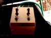
I now have 2 chips installed in my Casio SK8 - the original SK8 chip (the uPD43256), and the new chip (the DS1230Y), stacked on top of each other, with a switch and 2 resistors to switch between the 2 chips!!! Woooo Hoooo!!!!
This has given me 2 separate banks of 4 samples - the 4 from the original chip, and now an extra 4 from the top bank. Oh, joy, oh, joy!! 
It wasn't really hard to do at all, but there were things that I have learnt on the way that I will share with everyone, so that the journey is as smooth as possible.
I understand a lot more about digital electronics since I started on this project 2 weeks ago; I want to thank mi_dach especially for his priceless advice about address line connections and stuff, and everyone else who has helped with advice. Thanks, guys, this forum ROCKS!!!
I am going to start a new topic as a full write up, with pictures, on how to do the expansion. I feel that it is an important project, not because I wanted to expand my SK8, but because the procedure will enable you to expand pretty much ANY device that uses RAM memory to store programs, setting, etc.
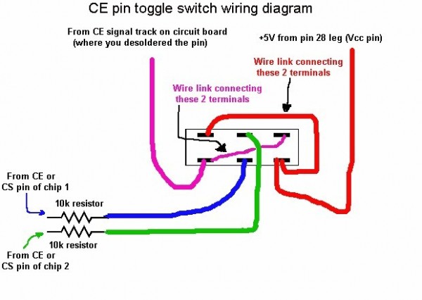
Just to leave you with something until I write it up, I simply soldered the new chip directly onto the old one, pin for pin, except for the CE pin (or CS pin on some chips), which I bent out horizontally away from the other pins on the new chip. I then disconnected the old chip's CE pin by de-soldering its track on the circuit board and isolating its pin. Please have a look at the datasheets for both of these chips first (they're a couple of posts up) and study them.
I then soldered 10k resistors to each of these CE pin legs of the 2 chips. These 2 resistors then went to the 2 centre terminals of a DPDT toggle switch via lengths of insulated wire - see the diagram below.
The rest of the wiring is as per the diagram. The CE signal track wire is soldered to the CE pin track on the track side of the board, anywhere near where you desoldered the CE pin from the original chip (make sure you don't accidentally reconnect the CE pin to the circuit track again).
The +5V supply wire is soldered directly to the exposed pin 28 leg (the +5V Vcc pin) of the original chip, as a convenient +5V supply for the switch.
That's basically it! Check out the full illustrated instructions in a new post soon. I'm off to play with my sampler expansion!! 
Cheers, Graham
| Description: |
|
| Filesize: |
51.2 KB |
| Viewed: |
580 Time(s) |
| This image has been reduced to fit the page. Click on it to enlarge. |
|
|
|
|
Back to top
|
|
|
Gimpoid
Joined: Jul 19, 2006
Posts: 5
Location: Ireland
|
| Posted: Wed Aug 02, 2006 9:18 pm Post subject:
|
|
|
well done graham mate i had every confidence in you..   |
|
|
Back to top
|
|
|
gmeredith
Joined: Jun 28, 2006
Posts: 82
Location: Tasmania, Australia
Audio files: 1
|
| Posted: Thu Aug 03, 2006 1:49 am Post subject:
|
|
|
I've just put up a new topic on how to do my memory expansion. It contains pretty well all the info needed. Please everybody read it and see if it makes sense, in case something stupid happened while I was typing!!
For those of you who think they might be smart and REMOVE the original chip and put an IC socket there, to make things interchangeable (this is what I DID) - DON"T DO IT!! There isn't enough clearance when the chips are stacked AND with a SOCKET, to get the circuitboard on.
You have to bow the board, like I'm having to do now, dammit, to get it to screw down in place. I only have just started putting it back together now, when I found out!
But if you do the expansion directly as in the instructions, leaving the original chip in place, you should have just enough clearance to put the board back in place and secure it without any stress on it. Just thought I'd let you know.
It actually is not an issue for me, because this mod was really only a test bed for me to try out and see if it worked; and it does, beautifully.
But I put a socket in, because I actually wanted to also try a BIGGER expansion later, which involves REPLACING (hence my use of the socket) the original chip with a bigger 8MBit chip directly, not stacking the chips, giving me 32x memory expansion! So this 2x expansion was really just an experiment. If I had planned on staying with just the 2x, I would have not used the socket. There would have been no point. With the 32x expansion, there is enough room for a socket and the big chip together.
Cheers, Graham |
|
|
Back to top
|
|
|
mi_dach
Joined: Dec 17, 2005
Posts: 133
Location: Sweden
|
| Posted: Thu Aug 03, 2006 2:34 am Post subject:
|
|
|
Hey!
glad to hear that it's working Congrats! Too bad about the socket not fitting with the stacked chips, I wonder if is there room for the socket and a single (larger) chip?
I'm curious to know, is it possible to toggle between the banks at any time (ie when it's playing some samples?) Can you quickly jiggle the switch back and forth between the banks without it crashing? |
|
|
Back to top
|
|
|
gmeredith
Joined: Jun 28, 2006
Posts: 82
Location: Tasmania, Australia
Audio files: 1
|
| Posted: Thu Aug 03, 2006 5:50 am Post subject:
|
|
|
Hi mi_dach!
There is lots of room for a socket and a single chip, i've already measured! Seeing my big 8MBit chip has arrived from the US today, I'll be attempting that expansion - 32x memory expansion! I'll really have to get the LED display happening in order to keep track of them!
I haven't tried toggling between the memories while it's playing yet. I'll try it when I get home from work tomorrow. Might make for some excellent sample mashing!!
Cheers, Graham |
|
|
Back to top
|
|
|
|

 Forum index » DIY Hardware and Software » Circuit Bending
